Features of high voltage input power module | 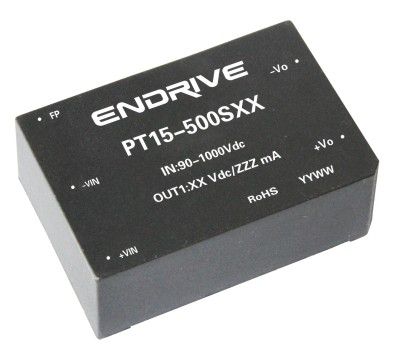
|
◆ Ultra-wide voltage input range: 90-1000Vdc
◆ Operating temperature range: -20-+85℃
◆ Complete protection functions (output short circuit, output overvoltage, etc.)
◆ Isolation voltage: 4000Vdc
◆ Small package, high power density
◆ High efficiency, ultra-low standby power consumption, energy-saving and environmentally friendly |
Application scope |
High-voltage input power supply modules are mainly widely used in supporting equipment such as photovoltaic power generation, busbars, wind and solar power generation, as well as high-voltage inverters. |
High voltage input power module model list |
Product model | Input voltage (VDC) | Output voltage (VDC) | Output current (mA) | Capacitive load (uF) | Efficiency (%, typ) |
PT15-500S05 | 90-1000 | 5 | 150-3000 | 4700 | 84 |
PT15-500S12 | 12 | 62-1250 | 2200 | 86 |
PT15-500S24 | twenty four | 31-625 | 1000 | 87 |
| * If you have any other specifications and models, you can contact our company directly. |
Input Features |
project | Test conditions | Min | Typ | Max | unit |
Turn on voltage |
|
| 85 | 90 | VDC |
MAX input voltage* |
|
|
| 1050 |
|
Standby power consumption | Input voltage range |
|
| 0.5 | W |
Input filtering |
| C |
Startup time | 500VDC nominal input |
| 2 |
| S |
Input current | 500VDC nominal input, rated load |
| 35 |
| mA |
Input current | 1000VDC high voltage input, rated load |
| twenty one |
| mA |
Input anti-reverse connection protection | built-in |
|
|
|
|
fuse | 1A/slow break, built-in |
|
|
|
|
*When using the input voltage exceeds this value, it will cause damage or damage to the product. |
Output Characteristics |
Output power | See output power Vs input voltage | 0.75 |
| 15 | W |
Output voltage accuracy | Input voltage range, 100% load |
| ±1 | ±3 | % |
Load adjustment rate | Nominal input, from 10% to 100% load |
| ±0.5 | ±1 |
|
Voltage adjustment rate | Input voltage range |
| ±0.2 | ±0.5 |
|
Cross-adjustment rate | 50% load on the main road, 25-100% load on the auxiliary road |
|
| ±5 |
|
Output overcurrent protection |
|
| 130 |
| %Io |
Output short circuit protection |
| Sustainable, self-recovery |
Output overvoltage protection |
| 110 |
| 140 | %Vo |
Transient response deviation | 25% load step change |
| ±2 | ±5 | %Vo |
Transient response time |
|
| 1 | 2 | mS |
Ripple & Noise | 20MHz bandwidth, nominal voltage input 100% load |
| 100 | 250 | mVp-p |
Switching frequency | Frequency modulation mode |
| 60 |
| KHz |
Temperature coefficient | Main Road | Nominal voltage input 100% load, -20℃~ +85℃ |
|
| 0.03 | %Vo/℃ |
| Auxiliary road |
|
|
| 0.15 |
|
General Features |
Insulation voltage | Input VS output, input and output VS housing, leakage current 5mA |
|
| 4000 | VDC |
| PT15-500EXXXX series, between two outputs |
|
| 1000 |
|
Insulation resistor | 500VDC test, 45-70%RH, 25℃ |
|
| 100 | MΩ |
Isolation capacitor |
|
| 2200 |
| pF |
Average failure-free time | MIL-HDBK-217F@25℃ | 200 |
|
| KH |
Thermal resistance | Device to housing (25℃) |
|
| 5 | ℃/W |
Housing material | Flame retardant and heat-resistant plastic, compliant with UL94V-0 |
|
weight |
|
| 120 |
| g |
Install | PCB |
|
|
|
|
Environmental characteristics |
Operating temperature | See product operating temperature derating curve | -20 |
| +85 | ℃ |
Storage temperature |
| -40 |
| 105 |
|
humidity |
| 5 |
| 95 | %RH |
Working Altitude | 5-85%RH, the product has no condensation and icing |
|
| 3000 | m |
The allowable housing temperature during operation |
|
|
| 95 | ℃ |
Pin soldering temperature | The solder joint is 1.5mm away from the shell, 10 seconds |
|
| 300 |
|
Cooling method |
| Natural air-cool |
vibration | GB/T2423.10-2008 |
Impact | GB/T2423.5-1995 |
注:1.以上所列数据除特别说明外,都是在TA=25℃,湿度<75%的条件下测得;
2.输出纹波噪声参考平行线测试法。 |
EMC特性 |
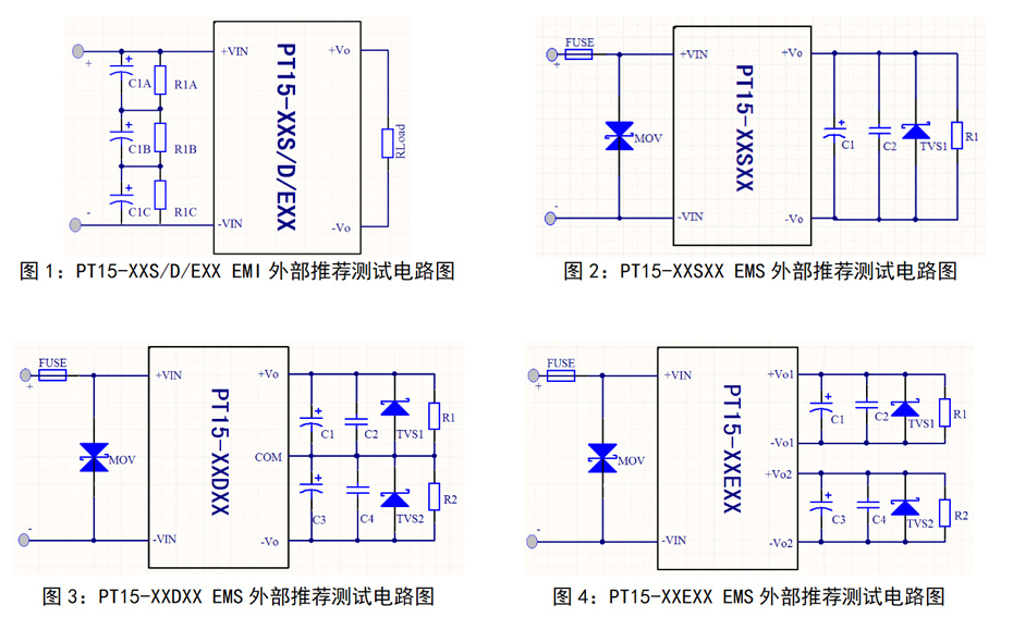
传导骚扰 | CISPR22/EN55022 CLASS A | 需外部推荐测试电路,见图1 |
辐射骚扰 | CISPR22/EN55022 CLASS A |
|
静电放电 | IEC/EN61000-4-2 ±4KV Perf. Ceriteria B |
|
群脉冲抗扰度 | IEC/EN61000-4-4 ±2KV Perf. Ceriteria B | 需外部推荐测试电路,见图2-4 |
浪涌抗扰度 | IEC/EN61000-4-5 ±2KV Perf. Ceriteria B |
|
|
参数说明 | EMI/EMS推荐电路和参数说明: 若需同时满足EMI和EMC特性要求, EMI和EMS推荐电路及参数可以电路叠加直接共用; EMS推荐电路中C1、C3为输出滤波电容,建议选取高频低阻电解电容。
|
器件 | 分类 | 规格 |
C1A-C |
| 47uF/450V |
R1A-C |
| 1MΩ/2W |
FUSE |
| 1A |
MOV |
| 142KD20 |
C2/C4 |
| 104K/50V |
TVS | 5V | SMCJ7.0A |
| 12V | SMCJ15.0A |
| 15V | SMCJ18A |
| 24V | SMCJ33A |
|
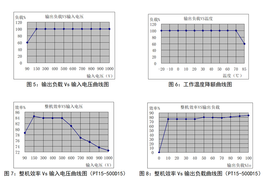
产品特性曲线 |
|
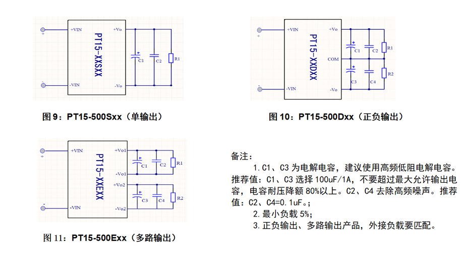
典型应用 |
推荐应用电路图:
|
外观尺寸、引脚方式 |
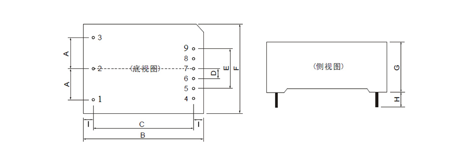
外壳尺寸(单位:mm) 注:端子截面直径:1.0mm 端子公差:0.1mm 其他公差:±0.5mm |